


Advertisement|Remove ads.
INTC Stock Jumps Premarket As Intel Takes Early Lead In ASML's Next-Gen Chipmaking Technology – Samsung, TSMC Are Next
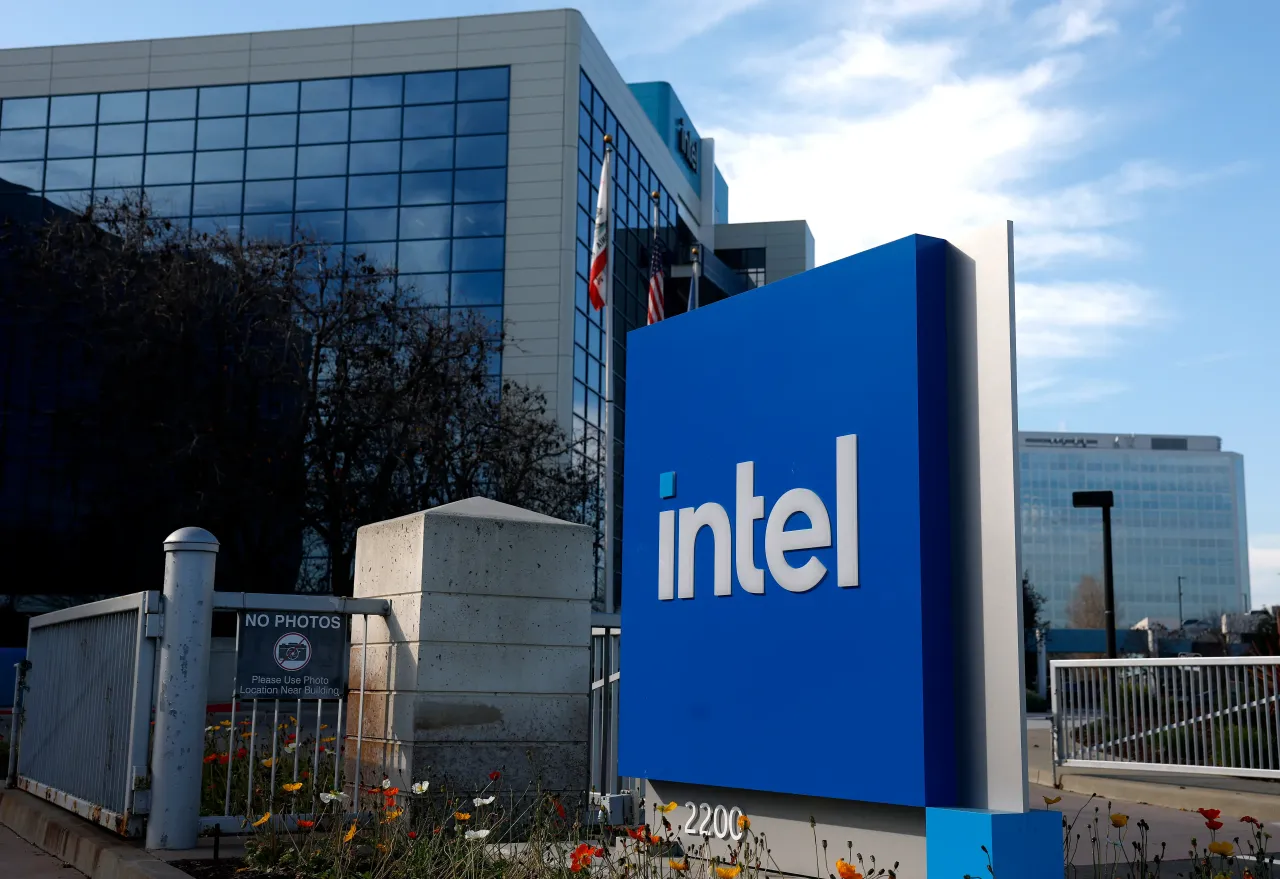


- Intel is already using ASML’s High NA EUV technology in high-volume manufacturing, with more than one million wafers processed.
- Samsung plans to introduce High NA EUV into high-volume DRAM manufacturing by 2028.
- TSMC plans to use High NA EUV in advanced-node, high-volume manufacturing starting in 2030 and expects the number of High NA layers to increase as AI-driven transistor architectures become more complex.
Advertisement|Remove ads.
Intel (INTC) and ASML (ASML) announced Monday that they have deepened their multiyear collaboration on High NA EUV lithography. Rivals Samsung and TSMC (TSM) are also lining up to adopt the technology, though on longer adoption timelines.
High NA EUV is a next-generation machine technology from ASML that helps chipmakers print smaller and more complicated features onto semiconductor wafers.
Intel is already using the technology in high-volume production, while Samsung plans to bring it into DRAM manufacturing by 2028 and TSMC plans to use it for advanced chips from 2030.
Advertisement|Remove ads.
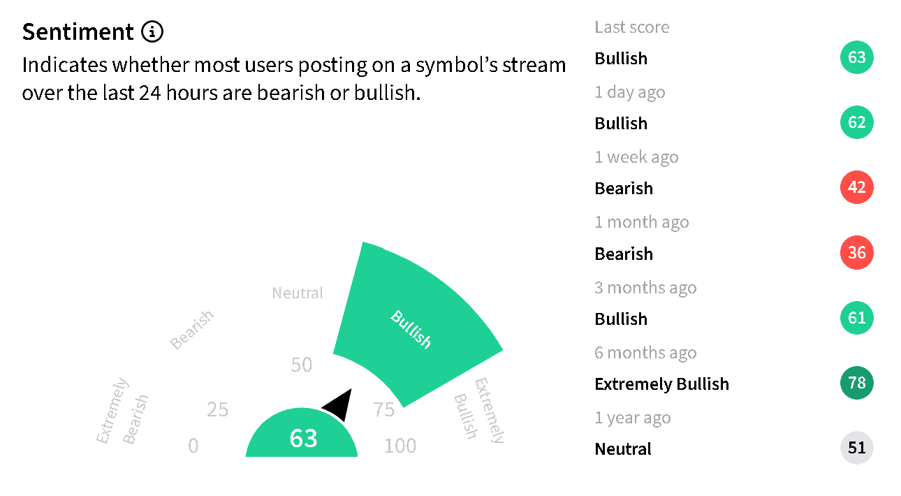
INTC stock jumped over 4% in pre-market trade and was among the top trending tickers on the platform. ASML stock rose nearly 3%, and TSM stock moved 1.5% higher amid weakness in the broader market. On Stocktwits, retail sentiment around INTC and TSM remained in ‘neutral’ territory over the past day, while sentiment around ASML trended in the ‘bullish’ zone.
Intel Is Already Using The Technology
Intel Foundry and ASML said more than one million wafers have now been processed using High NA EUV equipment. That includes testing and development work, along with actual production of some layers of Intel's Core Ultra Series 3 processors, code-named Panther Lake.
Intel said the machines are performing as expected in areas including accuracy, production speed and availability. It also said chips made using High NA EUV on its 18A manufacturing process are matching or exceeding the performance of comparable layers made using ASML's existing EUV technology.
Advertisement|Remove ads.
ASML CEO Christophe Fouquet called Intel "one of the key leaders of the industry's adoption of High NA," and pointed to its role in bringing the technology into commercial production.
Samsung And TSMC Are Getting Ready To Follow
Samsung plans to use High NA EUV for high-volume DRAM production by 2028. That would bring the technology into memory chips, rather than limiting it to advanced processors.
TSMC plans to use High NA EUV for advanced-node chip production starting in 2030. The company expects to need the technology on more layers of its chips over time as chip designs become more complicated, particularly for AI applications.
Advertisement|Remove ads.
Bigger Masks Could Make High NA More Efficient
Today, chipmakers use 6-inch masks, which are essentially templates that contain the patterns to be printed onto a wafer. ASML, Intel, TSMC, Samsung and other industry participants are working toward larger 12-inch masks.
The larger masks could allow chipmakers to print bigger areas of a chip at once. That could reduce the need to piece together different exposures, improve factory productivity, and lower manufacturing costs.
ASML and TSMC are targeting a pilot line for the larger masks by 2031, with the technology expected to be ready for advanced-node production by 2033.
Advertisement|Remove ads.
In the meantime, Intel and ASML are working on "reticle stitching," which allows chipmakers to use High NA EUV with today's 6-inch masks.
Read also: MSTR, COIN, CRCL Stocks Dip: Crypto Equities Pull Back After Bitcoin's $82K Rejection
For updates and corrections, email newsroom[at]stocktwits[dot]com.
Advertisement|Remove ads.
Comments posted here will also appear on symbol pages.

Latest News
/filters:format(webp)https://news.stocktwits-cdn.com/large_big_pharma_577fb207eb.jpg)
/filters:format(webp)https://news.stocktwits-cdn.com/IMG_8805_JPG_6768aaedc3.webp) Deepti Sri·9m ago
Deepti Sri·9m ago/filters:format(webp)https://news.stocktwits-cdn.com/large_Getty_Images_2245498698_eb56c3f1cc.jpg)
/filters:format(webp)https://news.stocktwits-cdn.com/IMG_9209_1_d9c1acde92.jpeg) Yuvraj Malik·53m ago
Yuvraj Malik·53m ago/filters:format(webp)https://news.stocktwits-cdn.com/large_elon_musk_jpg_a7dd779bcc.webp) Deepti Sri·1h ago
Deepti Sri·1h ago/filters:format(webp)https://news.stocktwits-cdn.com/Getty_Images_2293869390_1_fb85f04d83.jpg)
/filters:format(webp)https://news.stocktwits-cdn.com/shivani_photo_jpg_dd6e01afa4.webp) Shivani Kumaresan·1h ago
Shivani Kumaresan·1h ago/filters:format(webp)https://news.stocktwits-cdn.com/large_charles_hoskinson_OG_jpg_7eaff6116d.webp)
/filters:format(webp)https://news.stocktwits-cdn.com/Anushka_Basu_make_me_smile_in_the_picture_b92832aa_af59_4141_aacc_4180d2241ba8_1_2_png_1086e0ed8c.webp) Anushka Basu·9h ago
Anushka Basu·9h ago/filters:format(webp)https://news.stocktwits-cdn.com/large_Getty_Images_1922677353_03926a10de.jpg) Anushka Basu·10h ago
Anushka Basu·10h ago